
How AMD’s 3D V-Cache can amplify Ryzen performance by up to 25 percent
3D V-Cache will seem in AMD merchandise later this year.
At the present time’s Excellent Tech Deals
Picked by PCWorld’s Editors
High Deals On Colossal Products
Picked by Techconnect’s Editors
AMD mentioned Monday evening at Computex 2021 that it has superior its chiplet architecture into 3D chiplets, namely what it calls 3D V-Cache skills. By itself, the skills promises performance gains for its Ryzen and Epyc processors that can contact 25 percent.
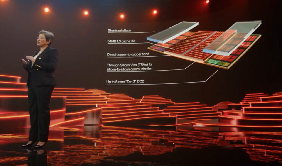
AMD has made “a lot development” on its 3D chiplet skills, and might well unbiased debut it in its “very most practical-stop merchandise” by the stop of 2021, AMD chief government Dr. Lisa Su mentioned at some point of a Computex keynote take care of.3D V-Cache enables AMD to rob a Ryzen 5000 mobile processor and fasten a 64MB SRAM cache straight on high of it.
Su showed off a Ryzen 9 5900X, AMD’s quickest gaming CPU, after which when in contrast it to a prototype 5900X with 3D V-Cache linked to it. In Xbox Game Studios’ Gears 5, frame rates improved by 12 percent. In other video games, also the train of an identically clocked 5900X, performance increased 4 to 25 percent, for an moderate of 14 percent, Su mentioned.
 YouTube / AMD
 AMD’s Dr. Lisa Su supplied benchmarks exhibiting how the prototype 3D V-Cache can dramatically make stronger gaming performance.
Stacked chips sound love the long term
This would well furthermore unbiased all sound familiar. In 2018, Intel started exhibiting off how its Foveros skills allowed for stacking its CPU good judgment on high of 1 one other. That allowed Intel to build the brief-lived Lakefield processor, but additionally the upcoming, higher-performing Alder Lake chip, which Intel displayed at Computex in every desktop and mobile variations.
 YouTube / AMD
 AMD CEO Dr. Lisa Su explains 3D V-Cache in her Computex presentation.
In step with Tirias Be taught analyst Kevin Krewell, on the opposite hand, AMD’s implementation of 3D stacking skills is rather a lot of. AMD is the train of through-silicon by approach of craftsmanship from TSMC, its foundry accomplice, an similar to the skills aged by memory makers to stack DRAM and NAND flash on high of 1 one other. It has higher energy and bandwidth characteristics than Foveros, on the opposite hand it’s unknown how successfully it could well furthermore unbiased also be manufactured.
“AMD is the train of the tech to find an extra ~12 percent performance enhance for its CPUs by including more L3 cache,” Krewell mentioned by approach of instant message. “This skills might also be aged in EPYC servers.”
Inserting a trim cache straight adjacent to the CPU can receive major performance advantages. Processors must count on for instructions, and storing them in an with out issues accessible cache—versus in quest of them out in machine memory—might well furthermore unbiased also be a easy methodology to amplify machine performance. Nonetheless baking that cache into the processor die introduces more opportunity for chip defects. In a worst-case convey, the full chip would be rendered unnecessary.
Adding the cache as a separate die after which stacking it saves condominium and worth, while tranquil declaring the bandwidth merit and including gobs of readily out there cache. To illustrate, Su mentioned its prototype soldered SRAM to every AMD CCD, for a entire of 192MB of SRAM cache. The readily out there level-3 cache on this day’s 5900X is ideal 64MB, or a 3rd of the 3D V-Cache prototype.
 YouTube / AMD
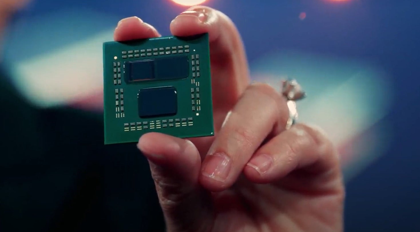
 AMD’s Su holds up the prototype 3D V-Cache chip.
Following AMD’s multichip modules and chiplet methodology, Su known as 3D chiplets the “subsequent wide step forward.” Inserting the extra silicon on high of the CPU die triples the readily out there cache. TSMC’s through-silicon vias (or on-chip “wires”) enable the CPU and cache to appear at with one one other at bigger than 2 TBps of bandwidth, Su mentioned. Su also mentioned that AMD’s die-to-die methodology makes train of divulge copper connections, now not solder bumps. That’s an oblique criticism of Intel’s Foveros methodology, which makes train of microbumps and thus consumes more energy and affords much less bandwidth, Krewell illustrious.
For now, that also skill that AMD can’t with out issues reproduce Intel’s Alder Lake methodology. Alternatively, it could well furthermore unbiased now not topic, as AMD can understand performance gains in every its Ryzen and Epyc processors, and presumably its GPUs. Now, the count on is: Which of AMD’s chips will doubtless be blessed with 3D V-Cache?
Repeat: While you have interaction something after clicking links in our articles, we might well furthermore unbiased build a miniature price. Learn our affiliate hyperlink protection for more crucial aspects.
As PCWorld’s senior editor, Note specializes in Microsoft recordsdata and chip skills, among other beats.