AMD triples Zen 3 CPU cache the employ of 3D stacking technology
cache money —
No longer a pipe dream—CEO Lisa Su demonstrated a working 3D-stacked 5900X prototype.
-
This exploded design shows an extra 64MiB of L3 cache atop the heart of the CCD, with structural silicon inserts to both facet of the novel layer.
-
AMD teased X3D packaging in its Financial Analyst Day about a months within the past, however the technology has reached manufacturing tell some distance more hasty than expected.
-
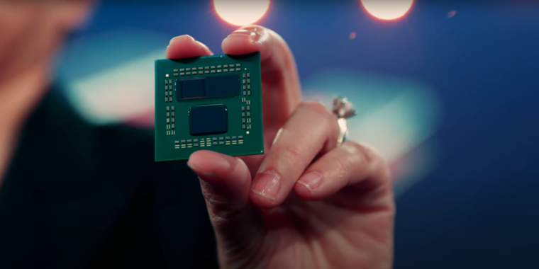
AMD CEO Lisa Su holds up a delidded, 3D-stacked Ryzen 5900x processor on stage at Computex 2021.
The day prior to this at Computex 2021, AMD CEO Lisa Su confirmed off the firm’s subsequent broad performance play—3D stacked chiplets, allowing the firm to triple the amount of L3 cache on its flagship Zen 3 CPUs.
The technology is appropriate what it sounds fancy—a layer of SRAM cache sitting atop the Advanced Core Die (CCD) of the CPU itself. Most modern Zen 3 structure integrates 32MiB of L3 cache per eight-core chiplet—making 64MiB total for a 12- or 16-core chiplet fancy the Ryzen 9 5900X or 5950X. The novel technology adds an extra 64MiB L3 cache on top of each and every chiplet’s CCD, bonded with thru-silicon vias (TSVs).
The extra 64MiB L3 cache layer does no longer prolong the width of the CCD, ensuing in a want for structural silicon to steadiness stress from the CPU cooling machine. Compute and cache dies are both thinned within the novel develop, allowing it to part substrate and warmth spreader technology with latest Ryzen 5000 processors.
-
Gaming workloads profit especially from extra L3 cache, as demonstrated by the 12% uplift going from 64MiB to 192MiB in this facet-by-facet demo.
-
Su claimed 15% average gaming performance uplift for the novel technology.
Tripling the L3 cache on Ryzen 5000 permits performance beneficial properties under some workloads—severely archive compression/decompression and gaming—same to these considered with entire novel CPU generations. AMD demonstrated performance uplift through a Gears of War 5 demo. Paired with an unspecified GPU and with clock bustle mounted at 4 GHz, a latest-mannequin 5900X machine completed 184 fps—whereas the triple-cached prototype managed 206 fps, a develop of roughly 12 percent.
AMD claims an average of 15 percent improved gaming performance with the novel technology, starting from a low of 4 percent for League of Legends to a excessive of 25 percent for Monster Hunter: World. This performance development requires neither smaller course of node nor elevated clock bustle—which is mainly attention-grabbing, in an period the place clock speeds maintain largely hit a wall, and a physics-obvious stay to course of-node shrink looks to be on the horizon as effectively.
Anandtech’s Ian Cutress notes that AMD’s novel 3D chiplet stacking course of is clearly TSMC’s SoIC Chip-on-Wafer technology in action. While AMD is—a minimal of to this level—limiting itself to two layers, TSMC has demonstrated a rotund 12 layers in action. The subject right here is thermal—in conjunction with RAM is a shut to-ultimate employ of the technology, since the extra silicon would no longer generate much within the procedure in which of extra warmth. Stacking CPU on CPU may maybe well be some distance more problematic.
AMD states that the redesigned 5900X will enter manufacturing later this 365 days—effectively before Zen 4’s scheduled initiate in 2022. For now, AMD is specializing within the novel technology for “excessive-stay Ryzen” CPUs totally—no mention used to be fabricated from Epyc, and the extra silicon required for the added cache makes it a doable nonstarter for funds processors, given latest materials shortages.
Listing image by AMD