IBM: One more chip within the wall
Tall Blue has developed technology it hopes will strengthen semiconductor traits for the next decade

By
-
Cliff Saran,
Managing Editor
Printed: 10 Might per chance per chance per chance per chance 2021 10: 45
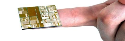
IBM has unveiled what it claims is a leap forward in semiconductor technology. Working with enterprise partners, the corporate sees no wall in semiconductor pattern that can well not be chipped away.
As more issues to find connected, there is increased inquire for chip performance and vitality effectivity. IBM said its newly developed 2 nanometer (nm) nanosheet technology helps come the cutting-edge work within the semiconductor enterprise, addressing this rising inquire. In accordance with IBM, chips developed the bid of 2 nm technology may per chance well beget 45% increased performance, or made to toddle 75% more vitality efficiently when put next with on the present time’s most developed 7 nm chips.
IBM vice-president of hybrid cloud research Mukesh Khare described the leap forward as a aspect of IBM’s research, which objectives to power semiconductor scaling to enhance the hardware required for hybrid cloud computing within the datacentre.
Researchers estimate that datacentres eat 1% of world electrical energy usage. In accordance with IBM, changing all datacentre servers to 2 nm-essentially based processors may per chance well potentially lower that quantity vastly.
Khare described the 2 nm technology as “foundational common sense”, which would meet the density, energy and performance requirements for common sense and memory chips, in both low-energy and excessive-performance applications.
Along side public and non-public sector enterprise partners, Khare said the semiconductor research at IBM’s semiconductor research centre in Albany, New York has the most likely to power chip technology for the next decade.
IBM works with loads of semiconductor partners to kit and produce the chips it designs.
In March, IBM solid a partnership with Intel to power semiconductor innovation. Such partnerships are considered as key to driving future traits in semiconductor technologies.
At the time, Dario Gil, director of IBM Analysis, said: “No single company, no topic how important, can to find and produce to come by the facility of many of those technologies on my own. IBM is a proponent of partnerships to scurry up innovation within the enterprise and has cultivated a thriving semiconductor research ecosystem in Albany, NY.”
He said the corporate has partnered with Samsung Electronics within the assemble of the IBM 7 nm chips, the first of that can come to market later this 365 days in IBM Power 10-essentially based systems. Gil said the collaboration with Intel would scurry up the scurry of packaging and job innovations into the future.
When asked if the semiconductor enterprise faces a wall, that can stop future breakthroughs, Khare said: “With the partnership now we come by and that quantity of skills and vitality, there’ s not a wall we are capable of’t fracture by.”
Software program areas for the technology vary from chips with 50 billion transistors to a handheld cell tool, with an estimated battery lifetime of four days, IBM said.
Manufacturing of semiconductors per the 2 nm technology is expected to launch up in 2024.
Assert material Continues Underneath

Learn more on Chips and processor hardware
![]()
IBM’s 2 nanometer CPU roadmap heats up chip manufacturer toddle

By: Ed Scannell
![]()
Crossbar ReRAM hits 1x nanometer job milestone

By: Carol Sliwa
![]()
Tall Blue sees 13th consecutive quarter of declining gross sales
By: Sean McGrath
![]()
IBM squeezes more out of chip technology with 7nm leap forward
By: Cliff Saran