It be not about soldered memory. It be in a roundabout blueprint about inserting RAM layers nanometers or microns…
The RAM standards are now transitioning to the DDR5 era that brings deal of improvements and substantial performance enhance when when put next with DDR4. On the opposite hand, DDR and its sooner GDDR relative need to not in fact that mercurial when when put next with the HBM (excessive-bandwidth memory) neatly-liked, which, in step with SK Hynix CEO Seok-Hee Lee, may perchance be the foundation for the natural merger between CPUs and RAM.
On the Institute of Electrical and Electronics Engineers’ Global Reliability Physics Symposium, Seok-Hee Lee offered his imaginative and prescient for a sooner memory neatly-liked that would require a “convergence of memory and logic.” Lee items a more slack evolution starting with HBM:
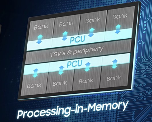
Because the velocity became once increased in excessive-bandwidth memory by rising the series of channels between the CPU and the memory, the velocity will elevate extra in Processing Attain Memory (PNM), where both the CPU and the memory exist within a single module. The velocity will extra elevate in Processing In Memory (PIM), where the CPU and the memory exists within a single equipment. In the extinguish, velocity will elevate extra in Computing in Memory(CIM), where the CPU and the memory is integrated within a single die, to express excessive performance computing blueprint.
SK Hynix is presently the 2nd largest memory maker on this planet, then again it does not derive another form of chips admire CPUs. Thus, CEO Lee requires a collaboration between semiconductor giants in bid to beget an ecosystem that can preserve the original CPU+RAM hybrids: “Handiest by setting up a strategic partnership for Originate Innovation in step with collaboration and sharing with possibilities, suppliers, academia and authorities, we are able to shape a original era, which pursues both economic and social fee.”
Lee also offered a original neatly-liked known as Compute Explicit Link (CXL) that would additionally complement the PCIe bus. The CXL memory is in a position to difficult data fleet and more efficiently between CPU and graphics / compute accelerators or good community interfaces. “CXL memory is being prepared as a solution that not handiest expands bandwidth and skill however also realizes the price of a persistent memory, […] one blueprint to narrow the gap between the memory performance and the industry necessities.”
Last however not least, Lee touched upon the efforts that are being made to strengthen the NAND memory chips integrated in SSD storage solutions. With the soar to 10 nm nodes and below, SK Hynix may perchance additionally at final be in a topic to assemble 600-layer NAND chips, which need to enormously elevate storage skill and data transfer speeds over the sizzling 176-layer cap.
Pick the SAPPHIRE NITRO Radeon R9 Fury with 4 GB HBM on Newegg