Processor, minute cost pumps construct a detrimental voltage
Launched in 1978, the modern Intel 8086 microprocessor ended in the x86 processors mature in most desktop and server computing at the present time.
This chip is built procedure digital circuits, as that that it’s possible you’ll well search recordsdata from.
Alternatively, it additionally has analog circuits: cost pumps that flip the 8086’s 5-volt present proper into a detrimental voltage to present a resolve to efficiency.1
I have been reverse-engineering the 8086 from die images, and in this put up I talk about the device of these cost pumps and how they work.

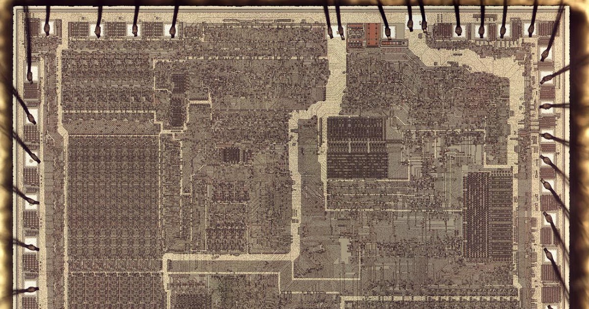
Die characterize of the 8086 microprocessor. The ALU and registers are on the left. The microcode ROM is within the lower spellbinding. Click for a high-resolution image.
The characterize above shows the minute silicon die of the 8086 processor below a microscope.
The metal layer on high of the chip is visible, with the silicon hidden below. Across the outdoors edge, bond wires connect
pads on the die to the chip’s 40 exterior pins.
Alternatively, careful examination shows that the die has 42 bond pads, not 40. Why are there two extra ones?
An built-in circuit starts with a silicon substrate, and transistors are built on this.
For high-efficiency built-in circuits, you could yell a detrimental “bias”
voltage to the substrate. 2
To abolish this substrate bias voltage,
many chips within the 1970s had an exterior pin that became connected to -5V,3
nonetheless this further vitality present became inconvenient for the engineers the utilization of these chips.
By the discontinue of the 1970s, on the opposite hand,
on-chip “cost pump” circuits had been designed that generated the detrimental voltage internally.
These chips mature a single helpful +5V present, making engineers happier.

A closeup of the 8086 chip exhibiting the silicon die and the bond wires connecting it to the lead body.
On the 8086 die,
the two extra pads feed this detrimental bias voltage to the substrate.
The characterize above shows the silicon die as mounted within the chip, with bond wires connected to the lead body that kinds the pins.
Having a see fastidiously, there are two small grey squares above and below the die; every connected to no doubt one of many “extra” bond pads.
The associated price pumps on the 8086 die generate a detrimental voltage, which passes by intention of the bond wires to those squares, and then by intention of the metal plate below
to the 8086’s substrate.
How the cost pumps work
The characterize below highlights the two cost pumps within the 8086.
I will talk about the discontinue one; the bottom one has the identical circuitry nonetheless a various layout to slot within the on hand space.
Every pump has driver circuitry, a mammoth capacitor, and a pad with the bond wire to the substrate.
Every pump is found next to no doubt one of many 8086’s two ground pads, presumably to lower electrical noise.

Die characterize of the 8086 microprocessor, zooming in on the two substrate bias generators.
That that it’s possible you’ll well per chance presumably additionally marvel how a cost pump can flip a obvious voltage proper into a detrimental voltage.
The trick is a “flying” capacitor, as shown below.
On the left, the capacitor is charged to 5 volts. Now, disconnect the capacitor and connect the obvious facet to ground.
The capacitor unruffled has its 5-volt cost, so now the low facet ought to be at -5 volts.
By all in the present day switching the capacitor between the two states, the cost pump produces a detrimental voltage.

On the left, the “flying capacitor’ is charged to 5 volts. By switching ground to the upper terminal, the capacitor now outputs -5 volts. (source)
The 8086’s cost pump circuit uses MOSFET transistors and diodes to change the capacitor between the two states, with an oscillator to govern the transistors, as shown within the schematic below.
The ring oscillator
consists of three inverters connected in a loop (or ring).
Since the amount of inverters is irregular, the map is unstable and can oscillate.5
For instance, if the input to the first inverter is 0, its output will be 1, the second output will be 0, and the third output will be 1.
This may per chance well well additionally simply flip the first inverter, and the “flip” will stir back and forth by intention of the loop causing oscillation.
To unhurried down the oscillation price, two resistor-capacitor networks are inserted into the ring. Since the capacitors will take some time to cost and discharge, the oscillations will be slowed, giving the cost pump time to operate.4

Schematic of the cost pump mature within the Intel 8086 to construct detrimental substrate bias.
The outputs from the ring oscillator are fed to the transistors that power the capacitor.
Within the first step, the upper transistor is switched on, causing the capacitor to cost by intention of the first diode to
5 volts with admire to ground.
The second step is the put the magic happens. The lower transistor turns on, connecting the
high facet of the capacitor to ground. Since the capacitor is unruffled charged to 5 volts, the low facet of the capacitor need to now be at -5 volts, producing the specified detrimental voltage. This goes by intention of the second diode and the bond wire to the substrate.
When the oscillator flips all another time, the upper transistor turns on and the cycle repeats.
The associated price pump gets its name because it pumps cost from the output to ground.6
The diodes are such as compare valves in a water pump,
making positive cost strikes within the spellbinding route.
The implementation in silicon
The characterize below shows the cost pump as it’s utilized on the chip.
On this characterize, the metal wiring is visible on high, with reddish polysilicon below and beige silicon at the bottom.
The predominant capacitor is visible within the guts, with H-formed wiring connecting it to the circuitry on the left.
(Section of the capacitor is hidden below the extensive metal vitality put at the discontinue.)
On the spellbinding, the substrate bond wire is attached to the pad.
A check sample is below the pad; it has a sq. for every cover mature to construct a layer of the chip.

The associated price pump, exhibiting the metal layer.
Taking out the metal layer shows the circuitry extra clearly, below.
The mammoth cost pump capacitor takes up the spellbinding half of of the characterize.
Despite the indisputable reality that minute, this capacitor is astonishing by chip requirements, regarding the size of a 16-bit register.
The capacitor consists of polysilicon over a silicon advise, separated by insulating oxide;
the polysilicon and silicon procedure the plates of the capacitor.
On the left facet are the smaller capacitors and the resistors that provide the R-C delay for the oscillator.
Below them is the oscillator circuitry and the flexibility transistors.7

An 8086 cost pump, exhibiting primarily the most basic substances. The metal has been removed for this characterize, to display cover the silicon and polysilicon below.
One titillating operate of the cost pump is the two diodes, every built from eight transistors in a standard sample.
The map below shows the structure of a transistor.
Regions of the silicon are doped with impurities to construct diffusion areas with desired properties. The transistor will likely be considered as a switch, allowing glossy to head with the stream between two diffusion areas called the source and drain.
The transistor is controlled by the gate, made from a various form of silicon called polysilicon.
A high voltage on the gate lets glossy stir with the stream between the source and drain, while a low voltage blocks glossy stir with the stream.
These minute transistors will likely be mixed to procedure common sense gates, the substances of microprocessors and other digital chips.
Nonetheless in this case, the transistors are mature as diodes.
 as implemented in an integrated circuit.")
Construction of an NMOS transistor (MOSFET) as utilized in an built-in circuit.
The characterize below shows a transistor within the cost pump, considered from above. As within the map, polysilicon kinds the gate
between the silicon diffusion areas on either facet.
A diode will likely be formed from a MOSFET by connecting the gate and drain together (facts)
by intention of the silicon/polysilicon connection at the bottom of the characterize.
The silicon can additionally be connected to the metal layer by intention of a “by intention of”.
The metal layer became removed for this characterize, nonetheless faint circles display cover the put of silicon/metal vias.

A transistor within the cost pump circuit. The polysilicon gate separates the transistor’s source and drain on either facet.
The map below shows how the two diodes are utilized from 16 transistors.
To attend the quite high glossy of the cost pump, eight transistors are mature in parallel for every diode.
Reveal that neighboring transistors portion source or drain areas, allowing transistors to be packed densely.
The blue strains display cover the metal wires; the metal became removed for this characterize. The darkish circles display cover connections (vias) between the metal and silicon.

The associated price pump has two diodes, every utilized with 8 transistors. The source, gate, and drain are indicated with S, G, and D.
Placing this all together, the upper eight transistors enjoy their sources connected to ground by a metal wire. Their gates and drains connected together by the polysilicon
below the transistors, making them into diodes, they typically’re connected to the capacitor by a metal wire.
The lower eight transistors procedure a second diode; their gates and drains are wired together by the lower metal wire loop.
Reveal how the layout has been optimized; shall we embrace, the gates enjoy crooked shapes to lead clear of the vias (gloomy dots).
Conclusions
The substrate bias generator on the 8086 chip9 is an enticing combination of digital circuitry (a ring oscillator formed from inverters) and an analog cost pump.
While the bias generator may per chance well well additionally simply seem love an obscure fragment of 1970s computer history,
bias technology is unruffled fragment of classy built-in circuits.
It is a ways intention extra complex in stylish chips which enjoy a pair of fastidiously regulated biases in a pair of vitality domains.
8
In a sense it’s analogous to the x86 architecture, one thing that started within the 1970s and is even extra smartly-liked at the present time, nonetheless has change into unimaginably extra complex within the seek for bigger efficiency.
At the same time as you are within the 8086, I wrote regarding the 8086 die, its die shrink assignment and the 8086 registers earlier.
I conception to analyze the 8086 in additional detail in future weblog posts so
apply me on Twitter @kenshirriff or RSS for updates.